Schematic Details, Pinouts and Technical Notes
This section describes the schematic notes. The description is divided into several generalized blocks that are thematically linked by their implementation or functionality.
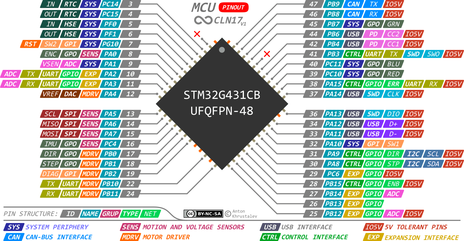
MCU
CLN17 utilizes the STM32G431CB - a high-performance microcontroller (MCU) based on the Arm® Cortex®-M4 core. Below is the pinout of the microcontroller.
User interaction
To interact with the user, two SPST PTS810 push buttons (SW1 and SW2) are utilized, which can be customized as per requirements. SW2 is connected to the NRST pin of the STM32 microcontroller and can be used for resetting the microcontroller as well as classic button. For indicating the operational status of the driver, a conventional 1515 RGB LED can be used.

External clock
For certain tasks, the presence of a reliable and accurate clock source for the MCU and RTC may be necessary. Although the STM32 microcontroller incorporates integrated LC resonators, they do not possess the same level of precision and linearity over temperature as crystals.
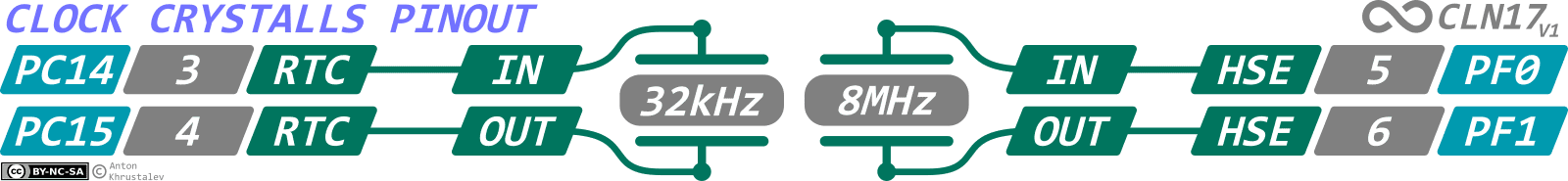
Hence, the CLN17 allows the provision of external crystals for LSE (Low Speed External) for RTC and HSE (High Speed External) for the System Clock. The LSE crystal should have a frequency of 32.768Hz (215 ticks per second). For HSE, the recommended frequencies are 8MHz or 12MHz.
USB Type-C connector with ESD protection
To enable communication with other devices using the USB 2.0 FS protocol, the board is powered by devices supporting PowerDelivery 2.0 via a 16-pin USB Type-C connector.

- 8 pins are used for power (4 for GND and 4 for VCC to withstand currents up to 5A)
- 4 pins are used for orientation-independent USB 2.0 (2 for D+ and 2 for D-)
- 2 pins, CC1 and CC2 (Configuration Channel), are used for PowerDelivery 2.0 communication via UCPD protocol on the STM32.
- 2 pins, SBU1 and SBU2 (SideBand Use), are used for SWD (Single Wire Debug) interface.
To protect the Type-C powering device from reverse polarity damage, an SS34B (D4) diode with a maximum continuous DC current of 3A is used.
To protect all USB Type-C interfaces, two 4-channel, low-capacitance, high-speed USBLC6-4SC (U6, U7) diode arrays are used (AN5612 recomendations). Since the USB, PD, and SWD interfaces are designed for voltages between 3.3-5V and frequencies up to 20MHz, these diode arrays are ideal. For the SWD lines, additional 100 Ohm resistors are used for additional protection against ESD transients.
SWD over SBU pins of USB Type-C
The 16-contact connector includes SBU contacts, which are rarely used for such a connector, except for Alternative Mode. Therefore, it was decided to use these contacts for a convenient programming interface that does not require specific wires and allows the device to be programmed without accessing the board.
SWDIO and SWCLK depend on orientation!
Not all USB Type-C cables have SBU lines, so it is recommended to use cables that support USB 3.1 or DisplayPort, as these cables guarantee the presence of these lines.
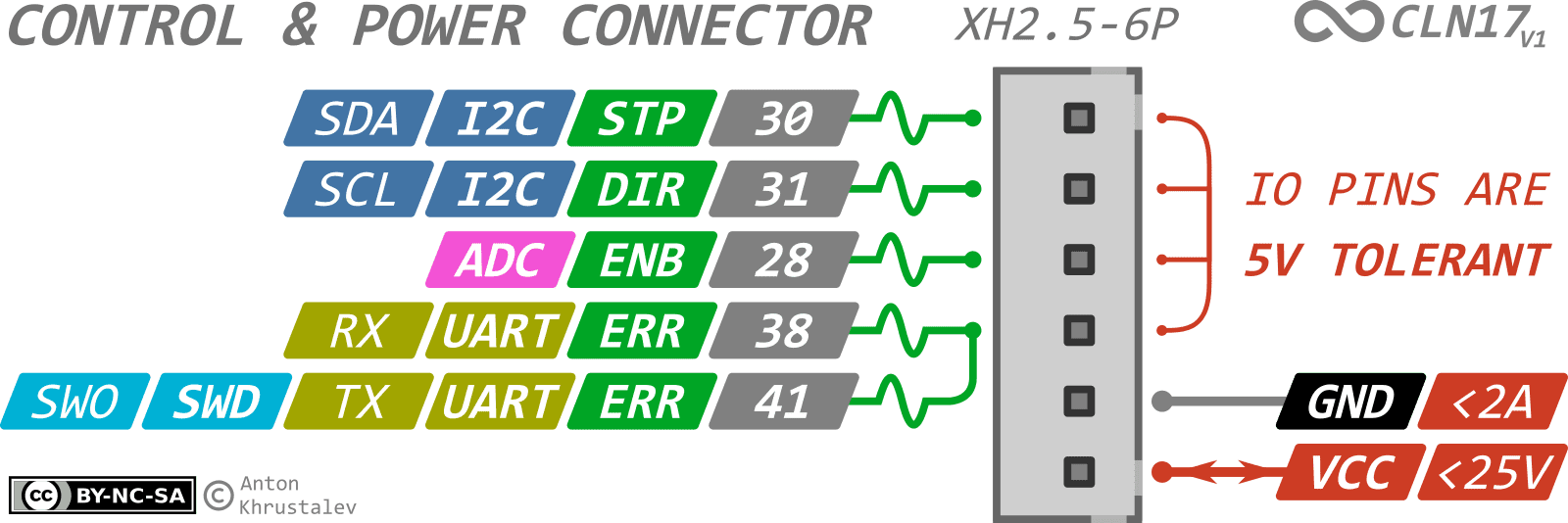
CONTROL Interface with ESD protection
To power and interface with the CLN17, three additional connectors are utilized.
PWR Connector: XH2.5-2P, which includes 2 power lines (VCC, GND). VCC is connected to the VBUS through a 1812 resettable fuse rated at 2A (maximum current depends on the ambient temperature). The 26V TVS diode SMBJ26A is used for protection against power surges. When paired with fuses, It also provides supply reverse polarity protection, causing overloading of the fuse and breaking the power circuit.
CTRL Connector: XH2.5-6P, which consists of 2 power lines (VCC, GND) and 4 signal lines. VCC is connected to VBUS similar to the PWR connector. The signal lines are tolerant to 5V and can be configured for PWM generation, digital input and output, or have the following functions:
- ERR can be used as an endstop or error signaling, UART Single-Wire for communication with the driver, and as an SWO output for SWD interface debugging.
- EN can be used for driver activation or as an analog input.
- DIR can be used for motion direction control or as SCL for the I2C interface.
- STEP can be used for motion control or as SDA for the I2C interface.
The general configuration for each output includes two series resistors with a nominal value of 100 Ohms. The midpoint of these resistors is connected to a voltage-limiting diode and pulled up to 3.3V through a 4.7kOhm resistor. This configuration offers several advantages:
- Limitation of the maximum IO current: For the STM32, it is set at 20mA, and the series resistors of 200 Ohms limit the maximum current to 16mA.
- Effective ESD protection: The series resistors reduce the load on the protective diode assembly, improving the suppression of strong ESD events. The first resistor limits the maximum peak current flowing through the TVS diode (150A at 15kV), thus limiting the voltage drop across the TVS diode (higher current results in higher voltage drop, VDROP). The second resistor limits the current from VDROP to the STM32 contact (1A at 100V), reducing the load on the integrated protection systems of the STM32.
- Short-term reverse polarity protection: When applying -5V to the contacts, the diode will limit the voltage to around 1V, and the resistor will limit the maximum current through the diode to approximately 50mA, preventing rapid overheating of the diode. The second resistor and the pull-up resistor ensure a decrease in the magnitude of the negative voltage at the input of the microcontroller.
- Pull-up to 3.3V for compatibility with both 3.3V and 5V logic and support for interfaces requiring pull-up, such as UART or I2C. The relatively high resistance does not interfere with the operation of 5V signals.
As protective ESD TVS diode used the 4-channel, low-capacitance, high-speed USBLC6-4SC (U5) diode array (as recommended in AN5612).
Maximum operating frequency of CTRL connector
It is important to consider that a series resistor, in conjunction with the capacitance of the circuit, creates an RC low-pass filter, which limits the maximum transmission frequency. The estimated capacitance of the topology elements does not exceed 40pF (4pF for the diode, 5pF for the STM32 IO, 8x2.5pF for each contact point on the circuit, 5pF for the connector, and 5pF for the PCB traces). As a result, the cutoff frequency of the filter (-3dB) will be close to 20MHz, so the estimated operating frequency will be close to 16MHz. However, it is necessary to take into account additional capacitance, resistance, and cable inductance (which depends on its length) that connects CLN17 with another device, as well as its own capacitance. Therefore, it makes sense to consider maximum frequencies up to 8MHz, with an optimal range up to 2MHz.
CAN-Bus driver with ESD protection
The CAN-Bus is implemented using the TJA1051 CAN-Bus driver as it supports CAN-FD (Flexible Data Rate) and enables data transmission at speeds up to 5MBit/s and It operates at 5V signal level.

However, any pin-to-pin compatible CAN-Bus driver can be used in place of the TJA1051. In most driver packages, the 5th contact of the SOIC-8 package is either VREF, VIO, or EN. The zero-ohm resistor (jumper) R25 must be installed for the VIO or EN option and not installed for VREF.
To protect against electrostatic discharge, an ESDCAN dual TVS diode assembly is used, which is not mandatory, but recommended for installation just in case.
For convenience in working with the linear topology of the CAN-Bus, the signal passes through the board from connector J5 to connector J6. Additionally, if necessary, jumper JP1 can be shorted to connect a 120-ohm termination resistor, in which case the CLN17 instance with the jumper installed will be the last element of the linear bus. Only two end devices (devices with a jumper installed or a termination resistor) should be connected to a single CAN-Bus.
Position and motion sensors
The Infineon TLE5012B used as high-precision magnetic angle sensor to determine the motor shaft position. The LSM6DSO IMU used as a 3-axis accelerometer and gyroscope to determine the driver's displacement based on acceleration and orientation.
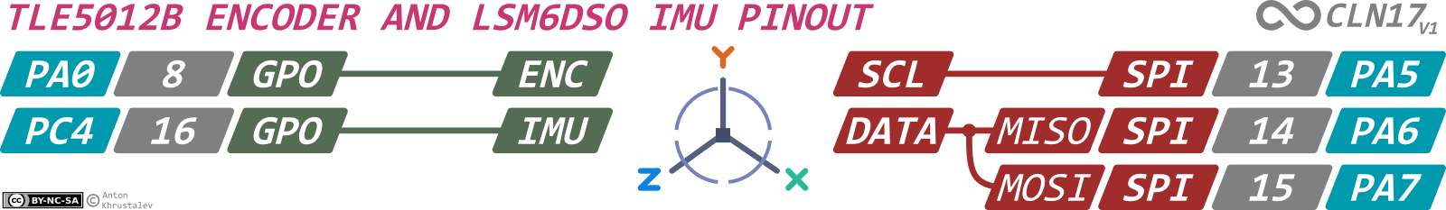
Both of these sensors are connected to the same Half-Duplex SPI interface (SPI 3-Wire). To achieve this, the MISO and MOSI pins on the STM32 are connected through a 510 Ohm resistor (R29). This resistor also helps to prevent circuit damage in case of collisions.
System power powering architecture
The CLN17 system powering architecture is designed to efficiently supply power to the MCU, Sensors, Logic Interfaces and CAN transceiver.

This is achieved by sequential cascading two voltage conversion stages, providing stable voltages for the various components. The voltage requirements for the MCU and the encoder are in range of 1.8 to 3.3V, while CAN transceiver with CAN-FD support requires a voltage range of 4.5V to 5.5V.
Stage 1: Synchronous DC-DC Converter (RY8310): Utilizing the RY8310 synchronous DC-DC converter, it allows for converting wide-range input voltage (VIN) into a constant 5V output voltage (VOUT) with high efficiency factor. If VIN is less than or equal to 5V, the converter maintains an output voltage close to the input voltage (VOUT ≈ VIN). The 5V output is used to power the CAN-Bus transceiver and 3.3V LDO.
Stage 2: Linear LDO Regulator (XC6206): Following the DC-DC converter, the second stage employs the XC6206 linear Low Dropout (LDO) regulator. This regulator converts the 5V output from the first stage into a stable 3.3V supply. This 3.3V voltage is then distributed to power the MCU, encoder and logic interfaces. Any pin-to-pin compatible LDO with VIN=5V and VOUT=3.3V can be placed
VSENS is used to measure system supply voltage (voltage divisor 10.2V/V or 8mV step with 12Bit ADC).
Stepper motor driver
CLN17 utilizes the bipolar stepper motor driver Trinamic TMC2209. It is designed for currents of 1.4ARMS per phase, 2ARMS per phase with a 50% duty cycle (period of 1s), and 2.8A peak per phase.
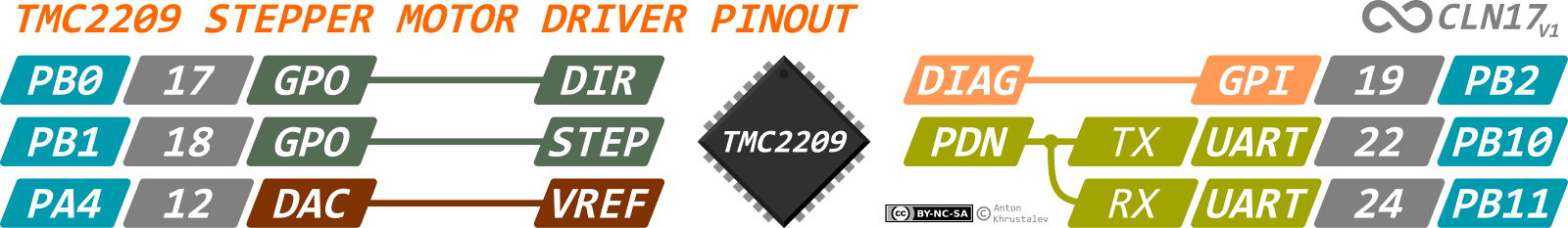
The driver is connected in UART mode, allowing it to be controlled by only three signal lines:
- DIR (responsible for movement direction);
- STEP (responsible for motor step);
- PDN (responsible for driver control). It uses the UART Single-Wire protocol, which enables data exchange over a single wire. Resistor R11 connected between RX and TX pins of the classic UART to implement UART Single-Wire support.
For more flexible and faster operation, two additional signal lines are connected to:
- DIAG pin (responsible for outputting the driver state). Can be configured to a certain level in StallGuard for fast detection of skipped steps or exceeding the current limit.
- VREF pin (responsible for the maximum motor current). Changing the voltage VREF by STM32 DAC in the range of 0-2.5V (recommended 1.25V-2.5V) changes the IFS system, that is, the maximum current of the coils can be in the range from 1A to 1.9A. Thus, VREF provides more precise current control for low-power operations.
CLK, MS1, MS2 and STDBY pins are pulled to ground for ease of routing (they are not used in UART mode).
XH2.5-4P connector is used as the motor connector, which has a current limit of 3A (more than the maximum coil current). A capacitor of 470pF is connected to each motor output (OA1, OA2, OB1, OB2), which increases the contact stability to ESD.